Table 3 Specifications Of LNA Design6 5. In case of CS stage use V DS V DD I Step 2.

Schematic Of The Proposed Lna Download Scientific Diagram
The die is packaged and mounted on the test board.
. Pad capacitance and parasitic capacitance of L B reduce input impedance Tail current source in diff-pair adds noise and common-mode instability. Design of a 10GHz LNA for Amateur Radio Operation Using AWR Software Cadence is a pivotal leader in electronic design and computational expertise using its Intelligent System Design strategy to turn design concepts into reality. Forty-five nm CMOS technology was chosen for the design.
Low Noise Amplifier also known as LNA is one of the most significant component for application in wireless communication system. Vonleo Member level 1. These factors are characterized by the design specifications in.
In this paper the same low noise amplifier from 1 is designed using Cadence Virtuoso tool to analyze the performance parameters. It is a very important part in RF receiver because it can reduce noise of gain by the amplifier when the noise of the amplifier is received directly. Power Consumption and Supply Voltage 2.
Welcome to the RF Design Tutorials video tutorial series. The attempt made in the paper shows an innovative designing for the enhancement and reliability in CMOS technology. Modeling Design Kits and the Cadence design flow are solid and accurate for RFIC design.
The lab is based on a Cadence SpectreRF Workshop session and its manual LNA Design Using SpectreRF previous called Application Note which is found on the course page. It is owned by Susan Nackers Ludwig and Eric Ludwig. Determine the J OPT of the amplifier.
The circuit is highly integrated with ESD protection circuits. Heterojunction Bipolar Transistor HBT LNA The design of the LNA is a cascode stage driving an emitter follower with a resistive feedback. Dec 9 2004 4 V.
The DC biasing voltage values for this design. Cadence System Analysis Key Takeaways The performance of an RF receiver is significantly influenced by the Low Noise Amplifier LNA. In this paper a low voltage CMOS LNA is designed for the GPS L1 band.
The proposed circuit of Cascode LNA was designed in Cadence Virtuoso 616 platform and simulated using the. A 24 GHz resistive feedback narrowband noise amplifier LNA using a series inductor input matching networks. Design Methodology for CS and Cascode LNA I Step 1.
Maintain this current density throughout the rest of the design steps. LNA is a small residential design firm specializing in projects around the Twin Cities area. To characterize the LNA following figure of merits are usually measured or simulated.
This research a LNA schematic consists of three stages which are common gate amplifier common drain amplifier and active inductor is designed to. LNA for the Bluetooth low energy BLE front-end circuit. Any Radio Receiver is made from Low Noise Amplifier mixer and Filter Power Efficient Active Filter where LNA plays a challenging role of amplificati on in the Radio Receiver Circuit.
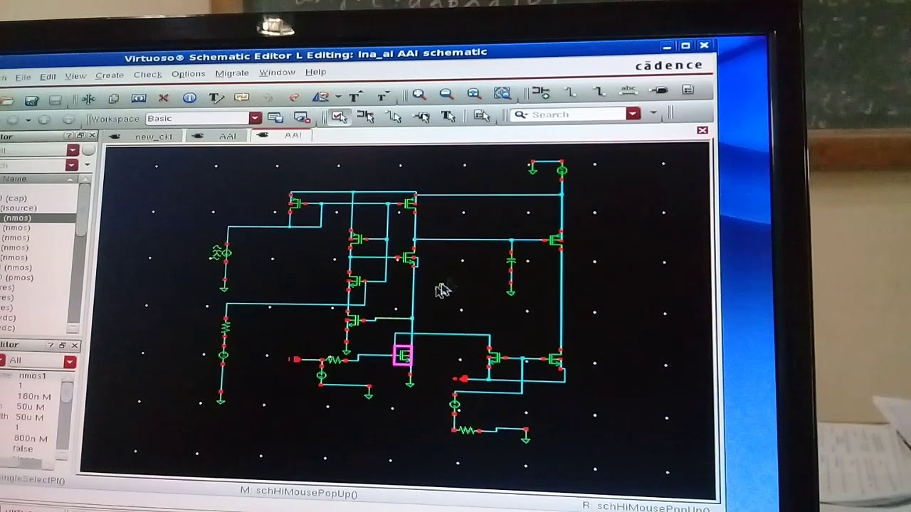
The schematic was implemented in Cadence Virtuoso Schematic XL using the generic processing design kit GPDK 45 nm library and was simulated using Analog Design Environment ADE. Lna design tutorial cadence The Cadence IC has a lot RFIC design examples. Start cadence by typing ams_cds tech c35b4 mode fb Make a new library RF_LAB1 in Cadence Library Manager Create and draw the Schematics.
RFDESIGN 2008 over 10 years ago. The supply voltage of 18V is given to the LNA. This is equivalent to solving.
Joined Oct 30 2004 Messages 34 Helped 1 Reputation 2 Reaction score 0 Trophy points 1286. In this paper we design and Simulate Low Noise Amplifier using Cadence Virtuoso R Schematic. DISCUSSION AND RESULTS Design and analysis of low noise amplifier is designed and simulated by using CADENCE software with latest technology 013µm.
The LNA presented in this. The cascode circuit is useful because it provides a larger gain and makes a stronger circuit. LNA design is a compromise among power noise linearity gain stability input and output matching and dynamic range.
The received signals are usually weak and noisy and they need to be strengthened before applying to the next stage. It is easy reliable with an extra g m boosting as well as inductively degenerated topology. In a receiver front-end a low noise amplifier needs.
Set the V DS of transistor for maximum linearity such that clipping of output is avoided. Design and analysis of low noise amplifier using cadence. Clarification on LNA design.
In the 9th video of the series you will learn about practical RF Low Noise Amplifier design flow. Any one help me that i am doing Complemetary current reuse LNA in MICS band in Cadence spectrai selected one IEEE paper regarding my projectIn that they didnot mention any device specification ie value of. The emitter follower is used as a buffer and provides more power and current to the circuit.
A Low Noise Amplifier is the basic building block or key component in the Communication System. Community Forums RF Design clarification on LNA design. Cadence customers are the worlds.
Design of Cascode LNA in 65nm CMOS BASAVARAJ P G1 NAGARAJ P2 DR SIVA YELLAMPALLI3. Look at the Cadence document and the example. Tuned LNA design notes MOSFET LNA design usually compromises noise figure for power dissipation low-noise current is too high In this approach linearity increases with Z O.
This requirement makes LNA an integral part of the receiver front end. Work is done one the Cadence virtuoso platform using the tsmc18 library. In this design the LNA operates at 26 GHz and a supply voltage of 18V is given.
Introduction A cascode low noise amplifier LNA at 2V power supply has been implemented in 018um IBM SiGe BiCMOS technology. They layout is also design with zero errors in both the Design Rule Check DRC and Layout vs Schematic check LVS implying that the design is ready for fabrication. LNA DESIGN USING SP ANALYSIS Starting with W f 1μm N f 80 Start with ballpark values for the inductors from hand- calculations First tune L Sto obtain R inreal part of ZM 1 close to 50Ω Next tune L Gto center S 11null at f 0 Tune L Dto center the peak of S 21at f 0 L G L S L D S-PARAM SIMULATION W f 1μm N f 80 L S 95pH L.
You will be familiar with the Cadence RFIC design tool. FminJ J 0.
2
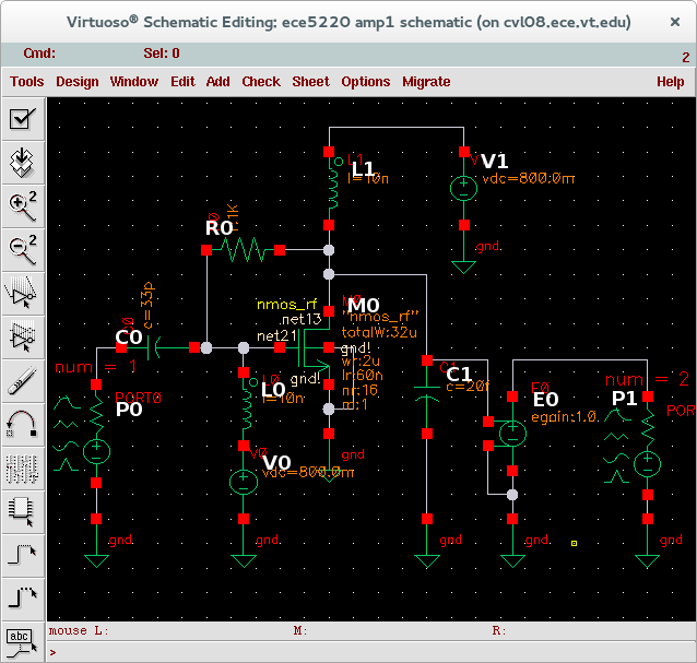
Linear Simulation For An Amplifier Multifunctional Integrated Circuits And Systems Group Mics Virginia Tech

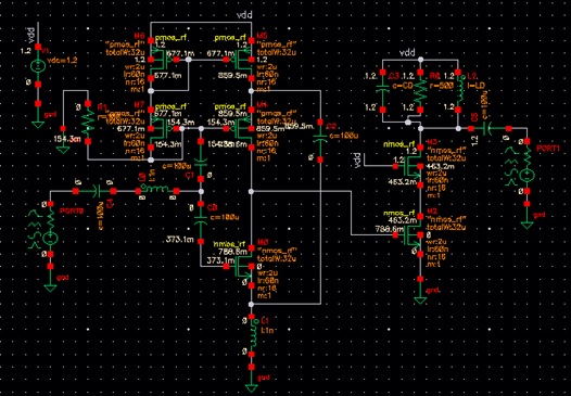
Figure 7 From Design And Analysis Of Low Noise Amplifier Using Cadence Semantic Scholar

Seeking For Help In Pss Analysis Rf Design Cadence Technology Forums Cadence Community
2
12 16ghz Lna
Design Of Cmos Current Reuse Low Noise Amplifier Using Modified Active Inductor Youtube

Figure 1 From Adaptive Enhancement Of Low Noise Amplifier Using Cadence Virtuoso Tool Semantic Scholar
0 comments
Post a Comment